Baking components to a PCB
The PCB passed all tests, so I sent it out for assembly. We’re paying another company to have a “pick-and-place” robot solder all the tiny components to our PCB. Some of the parts are just too small to do by human hands. Our FPGA’s pins are 0.8mm apart, and there’s 484 pins. Best to let a robot handle it.
While I’m waiting for the assembly to come back, I thought I would document how I tested one of the regulator circuits. Since I’m just testing the regulator circuit, we only have to solder the components in that circuit, not all of them (and certainly not the FPGA, phew).
Still, the components are very small (several 0402s which are 0.04in x 0.02in) and too small for me to use a soldering iron. There are some soldering iron ninjas that can do it, but sadly I’m not one of them.
Instead, I “baked” the components onto the board. This involves spreading tiny amounts of solder paste onto each of the PCB pads, carefully dropping the components on top, and putting the whole thing in the oven to reflow the solder. It’s like baking cookies, except much more precise and not tasty.
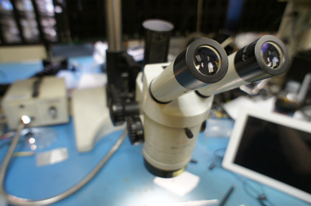
The first thing you need when baking PCBs is a good microscope. Here’s the one I used:
The second thing you need is a way of spreading solder paste in very small quantities. I use a sewing pin attached to a xacto knife base. It’s very precise and weighted well:
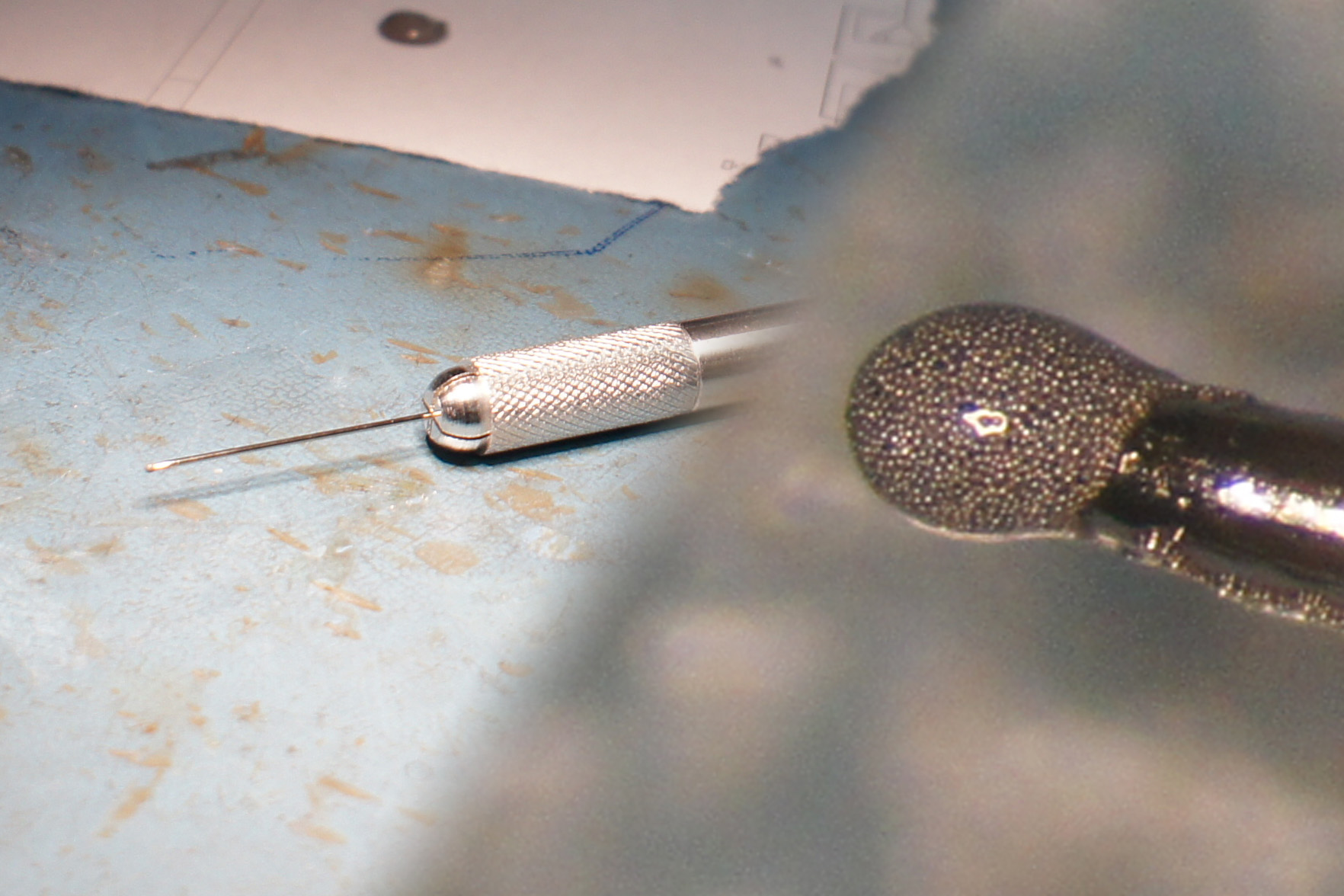
You can’t see it on the left, but there is a little drop of solder paste on the head of the pin. Looking in the microscope, you can see that the solder paste is just tiny spheres of solder suspended in some liquid.
The trick is to use the pin to spread the solder paste across each of the pads on the PCB. It took a few hours to get it just right for the regulator circuit I was testing. You need to make sure each pad is well covered, but not shorting out (connecting) to neighboring pads. The slightest movement becomes large under the microscope, so you have to calibrate your coffee intake just right. I’ve heard some labs keep a few beers around to keep a steady hand. Or so they say.
Once you’re done spreading solder paste over each pad, you VERY CAREFULLY drop the components on top. You have to be very precise, since a component that’s dropped incorrectly can short out pads and may require a lot of repainting. It sounds easy, but when you’re dropping 20-pin components with a pair of tweezers under a microscope, it’s a different beast.
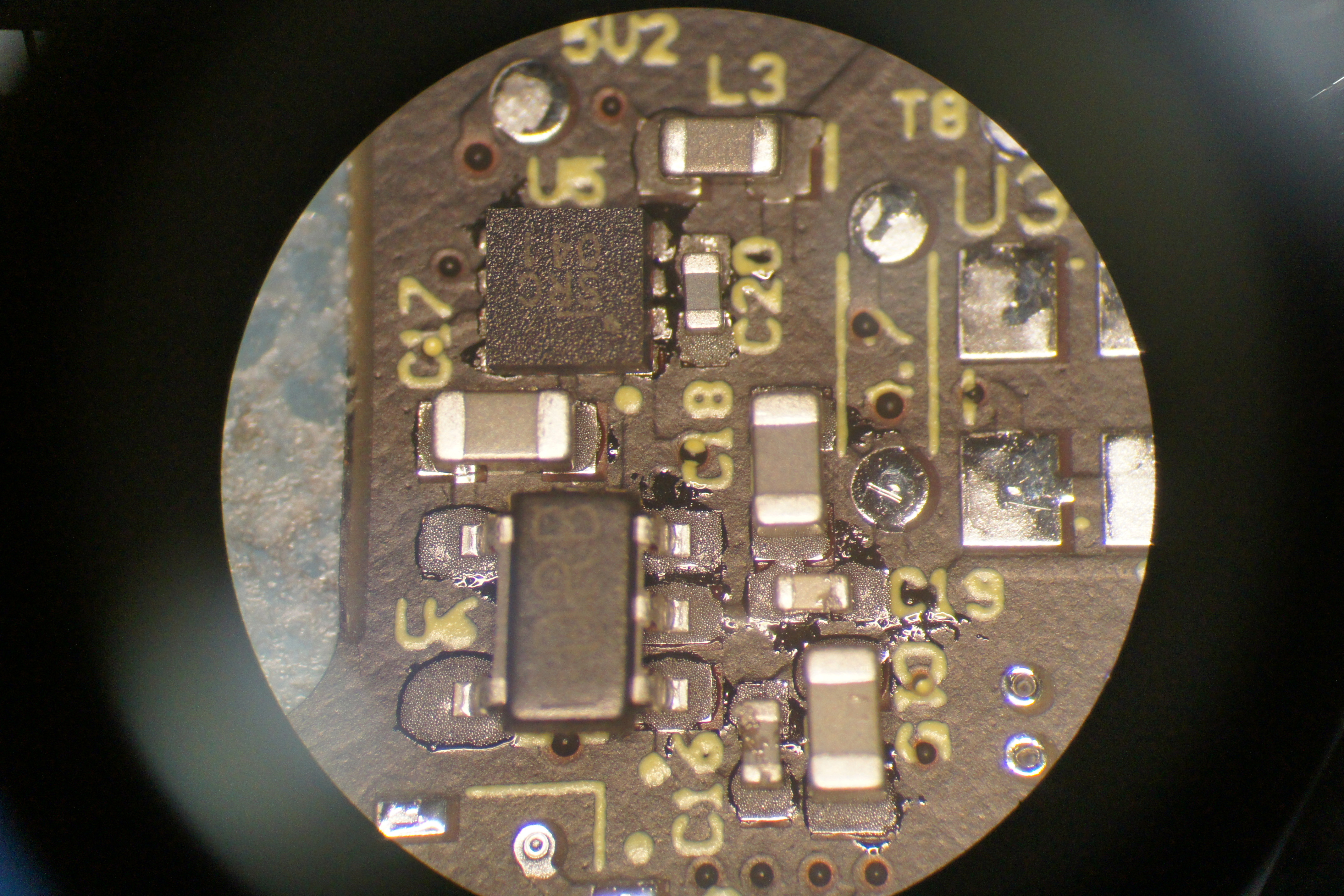
The photo above shows the result of the painting after dropping the components on top. Click the photo to see hi-res version.
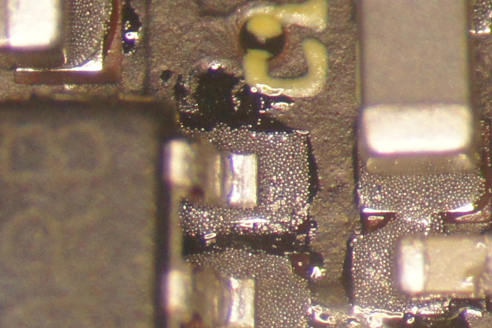
Here’s a zoomed in version above. You can see the spheres in the solder paste, and notice that there’s plenty on each pad. The trick is to get enough so that you’ll get good connections, but not so much that the pads short out. And don’t worry about the pads that look shorted on the right, they’re the same pad.
Once all of the pads are painted and the components are dropped on top, it’s time to bake the PCB. We have a special oven for this purpose, though it’s in Chinese so we just memorize which buttons to press in which order. You can specify the temperature profile, which specifies what temperature of the oven at various times. Some parts are sensitive to the profile, but we’re not using anything delicate and stuck with the default profile others have used.
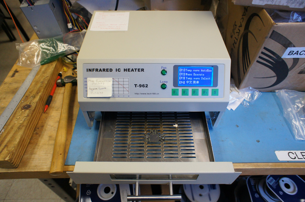
After eight minutes, the PCB was all baked:
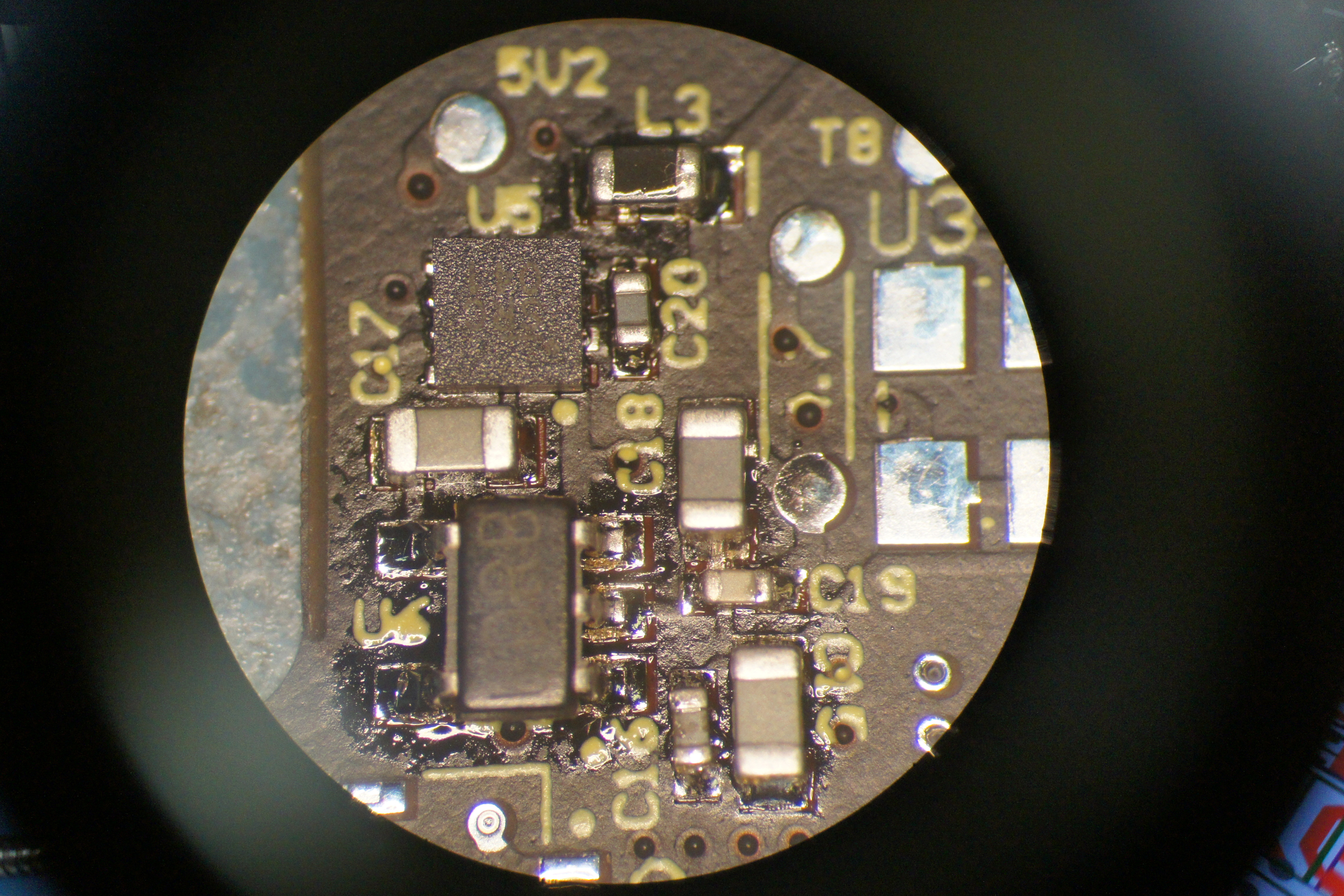
You can see the spheres in the solder paste have all melted together and now bond the component pins to their PCB pads. Click the photo for the hi-res version.
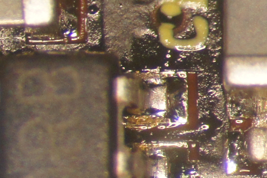
Here’s a zoomed in version:
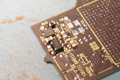
And lastly, here’s what the board looks like to the naked eye. Looks pretty good I think:
Once the board was fully baked, we then powered the regulation circuit and make sure it was generating the correct output voltage. Once it did, we knew the regulation circuit was working properly. Woohoo!